

Design Guidelines
Here are some general design rules that apply to all devices. If you plan to build your own device, you should follow these rules in your hardware and software design.
The most important goals are:
- keep it simple (complexity only when necessary)
- make it similar (differences only when necessary)
- make it easy to build up
- make it cheap
Network Topology
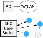
An SHC network consists of one base station and several other devices. The base station is the master of such a network. It communicates to every other device and controls it. It's connected to a PC (or router or NASNetwork attached storage This is a little box with one or more harddisks attached to your home network. Besides delivering storage space, a NAS usually has a descent processor running linux as operating system and supports a variety of additional services to run on the NAS. etc.) and serves as gateway to your normal home (W)LAN.
Network Topology
Every control mechanism the user wants to set up or change has to go through the base station. If devices communicate directly with each other (which is not forbidden), the possibility for the user to easily change the behavior is abandoned. Therefore, devices should only be designed to do so if reasonably necessary and configuration by the user is not needed.
Examples of possible devices with direct communication:
- A remote control which directly controls switches.
- A wall clock which gets the time from a DCF77The DCF77 longwave transmitter in Mainflingen, Germany sends out the official time in Germany since 1973. It can be received in a range of 1000-2000 km around the sender, covering western Europe. receiver device.
- A display which shows the status of other devices.
Generic PCBs
Different devices often need different PCBs, because of restrictions in size or form or to support different components, voltage levels and so on. Despite that, the number of different PCBs should be limited to the absolutely necessary amount to strengthen reusability, to reduce the development time for new devices and to reduce costs/time for producing PCBs.
The available devices use such generic PCBs if possible. PCBs should also be named like this (e.g. "Generic Midi" and not "Temp Sensor" PCB).
Please consider reusing or improving one of these PCBs for your new devices before you build up an additional special one.
ATMega Microcontroller
All devices are based on Atmel 8-Bit microcontrollers. Usually, an ATMega328 is used. It is available both in a 28-pin PDIPDual in-line package This is the typical form factor of ICs with pins. The pin pitch is usually 1/10 inch. PDIP means "Plastic DIP". package (1/10 inch pin grid) and as 32-lead TQFP(Plastic / Thin) Quad Flat Package This form factor is used typically for SMD ICs. Pins are at all sides of the package and can be soldered directly to the PCB. (SMD) package.
The ATMega168 has less memory. If its RAM, EEPROM and FLASH size is sufficient, this model could be chosen. But as the price is pretty much the same, the ATMega328 is to be preferred in general. Please also make sure to provide some reserves for improvements when choosing the microcontroller model. A smaller version than the 168 does not make sense, because the firmware wouldn't fit into it.
| Model | Flash | RAM | EEPROM |
|---|---|---|---|
| ATMega328 | 32 kB | 2 kB | 1 kB |
| ATMega168 | 16 kB | 1 kB | 512 Byte |
Memory sizes of ATMega328 and ATMega168
RFM12B Wireless Communication Transceiver

RFM12B
transceiver
For wireless communication between devices, the RFM12B ISM band transceivers from HopeRF are used at a frequency of 868 MHz. These transceivers are cheap and have a very low power consumption. They can also wake up the microcontroller at a programmed time, so it can be set to a low power sleep mode.
There are different types of this transceiver with different operating voltages (see table). They have some minor differences and the RFM12 without "B" is the older model. For compatibility reasons, I chose to use the RFM12B only, so the source code and the hardware schematics can be the same for all devices. The RFM12B has also better output power and reception performance as well as a "Synchron pattern Command". By using it, one could filter out packets from other SHC networks easily without decrypting packets first.
| Model | Operating Voltage |
|---|---|
| RFM12 | 2.2..5.4V |
| RFM12B | 2.2..3.8V |
| RFM12BP | 3.3V / 12V |
Operating voltages of different RFM12 models
Controlling the Power Supply of the RMF12 module
RFM12 modules seem to be unstable over longer time to receive messages when they remain in receive mode (actively listening). My experience is that most modules are not receiving any messages anymore after several weeks or months of constant use. To cover this situation for such SHC devices, the power (VCC) pin of the RFM12 module is controlled by the ATMega. This allows automatic resolution of this error condition by restarting the RFM12 module. The RFM12 module also has a software command for resetting and a hardware reset line, but switching off the module completely for a short time is the safest option.
The RFM12 could be directly connected to an ATMega I/O pin as the power source. But it is better to use a transistor to switch a clean VCC signal. The reasons: The RFM12 needs at least 2.2V. The ATMega is powered at VCC of 3.3V in many cases (e.g. Power Switch). The max. continuous current for the ATMega I/O pin is specified as 30mA, but the RFM12 already needs 27mA when sending. The ATMega I/O pin also has a voltage drop of about 1V or more at this high current, and therefore might have temporarily too low voltage for the RFM12. Look for "I/O Pin Output Voltage vs. Sink Current" in the ATMega's datasheet if you want to read the details. Therefore it's recommended using the additional resistor and transistor as it is implemented in the Base Station or Power Switch V1.3+.
One additional thing to consider is the value of the capacitors. There is a capacitor "before" the transistor that switches the RFM12 module, and there is one after it. Additionally, there are capacitors on the RFM12 board. Assume the first capacitor is 10µF and charged at VCC 3.3V, the 2nd is 1µF and at 0V (RFM12 switched off), and then the transistor switches. In this moment, the 10µF capacitor decharges to the 1µF capacitor and the RFM12 internal capacitors instantly, and the VCC drops. As the power source for the 3.3V is a small LP2950 voltage regulator, it also doesn't deliver so quickly the needed voltage to compensate this effect. You can see in the following diagram, that the VCC drops shortly down to ~2.26V. Using the usual BOD (undervoltage) level of 2.7V for the ATMega, it would now reset. An endless loop of resets is the result. This is not a theoretical problem, but I had this issue for real. When the first capacitor is 100µF instead, the voltage drops shortly only to 3.13V, which is safe for the ATMega to not reset.
Note: The BOD level can only be set to certain values. The one below 2.7V would be 1.8V. But this is too low for the ATMega to run safe at 8MHz, as it is configured in the Power Switch. Therefore it's not a good option to set the BOD level down to 1.8V.
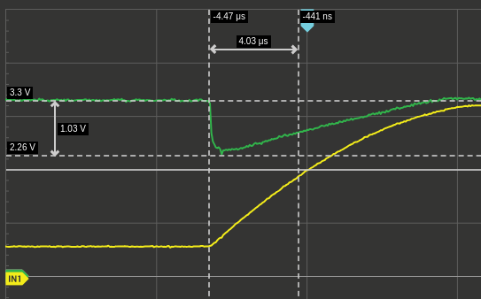
Voltage drop when switching on RFM12 over transistor with 10µF cpacitor (green: VCC before transistor, yellow: VCC at RFM12)
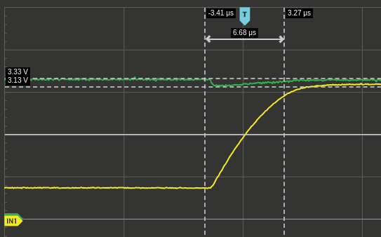
Voltage drop when switching on RFM12 over transistor with 100µF cpacitor
For details on how the Transceiver Watchdog function works to power the RFM12 module, read here.
Operating Voltage
The ATMega168/328 has an operating voltage range of 1.8 to 5.5V. Many devices are designed to be used with batteries (alkaline cells with nominal voltage of 1.5V). To allow operation with only two cells up to their minimum lifetime voltage of ~1V, the microcontroller can run at just 1 to 4 MHz. If this speed is not enough or other components with a higher minimum operating voltage are involved, think about using a step up DC-DC converter to allow operation with only two cells. On the other hand, if size or weight is not an issue, using three or four batteries may be the easier solution.
A simple sensor device typically uses AAA (micro) cells. You should choose a battery type which allows an operation of the device for at least 5 years without changing batteries.
The RFM12B transceivers have an operating voltage range of 2.2 to 3.8V. This gives us the possibility to either run microcontroller and transceiver using the same power supply with a microcontroller speed up to 4 Mhz, or to use a separate voltage of 5V for the microcontroller, which then requires I/O pin voltage level conversion between these parts.
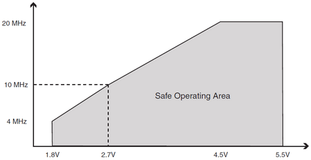
Possible clock speeds at different voltages (from Atmel datasheet)
| Configuration | Voltage | Level Conversion | Speed |
|---|---|---|---|
| 2x battery | 2.2..3.0V | no | 1..6.5536 MHz |
| 3x battery | 3.0..4.5V | yes | 1..12 MHz (*) |
| power supply | 3.3V | no | 1..12 MHz |
| power supply or >3 batteries | dual 3.3V + 5.0V with voltage regulator | yes | 1..20 MHz |
Typical operating voltage configurations and possible clock speeds, (*) 11.66 Mhz would be the maximum at 3V according to the diagram, so 12 Mhz is 3% overclocked
Clock Sources and Processing Speeds
As clock source, the internal RC oscillator is used whenever sufficient. It runs only at 1 MHz or 8 MHz and can be calibrated to improve the accuracy for e.g. using the serial port. The SHC's RC oscillator calibration function can be used for that.
There are three reasons to use an external crystal instead of the RC oscillator:
- The only possible speed of 1 MHz is not enough at a device with 2 battery cells.
- A speed above 8 MHz is needed.
- A lower drift of the clock speed caused by changed temperature or over time is needed.
If none of these reasons apply, use the internal RC oscillator.
One-sided PCB Layout
If PCB size is not an issue, the PCB of a device should have most circuit tracks on one side. That means it is mostly a one-sided layout and only a minimum amount of additional PCB tracks is on the 2nd side. This makes etching (at home) of the PCB much easier, because true two-sided PCBs (with many circuit tracks also on the 2nd side) require exact positioning of the mask. Few connections on the 2nd side can be realized using simple wires instead of etching a two-sided PCB.
For producing a PCB professionally, a (true) 2-sided layout may be the right choice, because the PCB can be smaller. But this should only be considered as an option if the 1-sided layout is already developed.
Fuses
The fuse bits (or "fuses") are configuration bits for the microcontroller that cannot be changed by the firmware. There are three such
bytes: the low, the high and the extended fuse byte. The most important fuses for most devices are for the clock source and the EESAVE bit,
which configures that the EEPROM memory is preserved through the chip erase. This is useful for development, because the device configuration
in the EERPOM needs not be flashed every time the chip is erased. In any case, all fuse bits are defined in the fuses.c file of any
device firmware. You can flash the fuses by calling make program_fuses.
| Fuse | Description |
|---|---|
| CKSEL0..3 | clock source selection |
| CKDIV8 | divide clock by 8 |
| EESAVE | preserve EEPROM memory through chip erase |
Some important fuse bits (read Atmel documentation for details)
6-pin ISP Connector
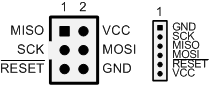
6-pin ISP and mini ISP pinout
The ISP (In-System Programming) connector is used to flash the firmware to the microcontroller while it is already inserted into the target system. This is the most typical use case for flashing a microcontroller in the development phase.
For the connection, the standard Atmel 6-pin ISP connector with 1/10 inch (2.54 mm) pin pitch is used, following this application note from Atmel. If this connector is too big for a device (especially on small SMD PCBs), use the smarthomatic mini ISP connector instead, which has 1/20 inch (1.27 mm) pin pitch.
The VCC pin is not connected by default. This is because the behavior regarding the VCC pin is different at different programmers. Some need the VCC line to detect the operation voltage from the circuit to allow programming, some provide a voltage on that pin to power the circuit and some simply ignore the pin. A short circuit and damage to the programmer or SHC circuit has to be avoided, so the VCC pin is not connected in most PCB layouts or may only be connected by a solder jumper.
USB-to-Serial Converter
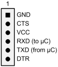
6-pin USB-to-serial pinout
Some devices may need a permanent connection of serial I/O to communicate with a PC. This is especially the case for the base station. A USB-to-serial connector / board not only allows communication with a device, but can also provide power. Please use a device with Arduino LilyPad compatible pin layout like the FTDI Basic Breakout board from DFRobot. This board type is produced by many companies and should be easy to get. One could solder an appropriate USB-to-serial IC like the FTDI FT232RL directly to the SHC device's PCB, but because the pin pitch is very small it is much easier to use a prebuilt breakout board.
UART Debugging Connector
An SHC device should have a UART output (TX) pin for debugging. You can connect this with a MAX232 (or compatible) level converter to your PC's RS232 serial port or to a USB-to-serial converter. You can debug the device firmware easily in the development phase by using a simple terminal software.
When using a 1 MHz clock speed or if you only use the UART for debugging, use 4800 Baud, no parity, 8 data bits, 1 stop bit. For higher clock speeds, especially when using a crystal, use 19200 Baud where necessary.
Connector for Optional I/O Pins
Whenever free space on the PCB allows it, add some additional port pin headers. Even if these are placed distributed around the PCB, it makes it very easy to extend a device with additional sensors, actuators or debugging parts and does not make the PCB bigger usually. Preferably the TX and RX pin, the interrupt inputs, the PWM outputs and such special purpose pins should be made accessible.
Status LED
Every device should have one status LED for the easiest form of debugging. The LED should preferably be connected to port pin PD7. This port pin has no special ability for which it could be used otherwise. It is also easier to understand to always use the same pin on all devices if possible.
Reset Button
A reset button is not needed in most cases, because the device can be restarted by disconnecting the battery or by flashing the firmware.
Why not use Arduino boards
Generally speaking, SHC devices should be simple in their hardware layout as well in software design and should not have unnecassary demands to the developer (or development environment). Using Arduino boards (or making SHC devices Arduino compatible) would contradict to that, because this would add these constraints (specific pinout or hardware specifics, firmware parts, development environment etc.).
The problem with using a typical Arduino board is also the price and that they are not specifically designed to be used with a wireless transmitter like the RFM module. If you would buy an Arduino board and a shield with a RFM12 (or other) transmitter, it would cost you much more money than a small PCB specifically designed for this purpose.
Another problem is power consumption. The bigger Arduino boards are not powered directly by batteries, but convert the voltage first, which wastes power (= battery lifetime). You could use an Arduino LilyPad and directly solder a battery to it. The problem is, that again you need to connect the RFM12 module somehow, and this is not easily possible with this board.
As a summary, there may be some use cases where using an Arduino board without the need to solder something may be an easy solution. But as an end product, I think this cannot be the right choice because of size, cost, battery lifetime and unnecessary restrictions in general.
License
Different licenses are used for smarthomatic:
Hardware

All hardware files (schematics and layout) are stored under the "hardware" subdirectory of the Git repository and are copyright (c) 2013 Uwe Freese, licensed under the Creative Commons Attribution-ShareAlike 3.0 Unported (CC BY-SA 3.0). This means:
- You can copy, distribute and transmit the work, but only without restriction under the same license.
- You can make commercial use of the work.
- You have to attribute a changed version by naming the original author. You have to make clear what you changed.
The physical hardware produced by using the hardware files is not covered by this license. It can be modified, produced and sold as you wish to.
Firmware Source Code
All files not in the hardware subdirectory of the repository belong to the firmware. It is licensed under the GNU General Public License (GPL) V3.0 and above. This allows anyone to:
- use the software for any purpose.
- study the source code to find out how the program works.
- distribute the software to others without restriction under the same license.
- change and improve the software and to publish the changes, as long as the changed version is also under the same license.
Please read the complete GPL license for details.
Homepage and Logo
The smarthomatic homepage (this website), the smarthomatic logo (the "house") and logotype are copyrighted (c) by 2013 Uwe Freese. They may only be used under restrictions as described in the impressum.
Wiki

The content of wiki is created by the community. It is licensed under the Creative Commons Attribution-NonCommercial-ShareAlike 3.0 Unported (CC BY-NC-SA 3.0).
Golden Rules
Here are the golden rules for designing an SHC device:
- Control devices only by the base station if possible.
- Use an ATmega328.
- Use the RFM12B transceiver for communication.
- Use few and small standard battery cells that allow an operation of at least 5 years.
- Use the internal RC oscillator at 1 MHz or 8 MHz if sufficient.
- Support the RC oscillator calibration function.
- Create a one-sided PCB with THT technology, and only SMD when necessary.
- Use the fuses.c file to define fuse settings.
- Use the standard 1/10 inch 6-pin ISP connector, or the 1/20 inch 6-pin mini ISP if necessary.
- For the connector of a USB-to-serial board, use the pinout of the Arduino LilyPad.
- Support a UART TX pin at 4800-1N8 configuration for debugging.
- Add some pin headers for I/O pins when PCB space allows it, especially for port pins with special ability.
- Support the status LED at port pin PD7.
- Respect the licenses.