Table of Contents
Building up a Power Switch
Needed Parts and PCB
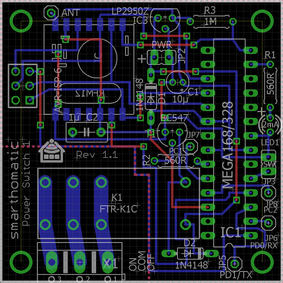
You need a PCB. You may use the layout from Github and etch it yourself or let a company produce one for you using the layout.
Partlist (in buildup order)
maybe extra pins, at your opinion.
Buildup of PCB
As always: start from flat to high. Go through the partlist and solder the parts from the top ones to the last ones.
For some parts, you have to consider something special:
- IC holder: Look at the notch and place it in the right direction.
- LED: Solder it to a wire if you want to place the PCB in a housing later. Read the instructions on how to solder the LED to a cable. The longer wire of the LED is +. It goes into the hole more in the middle of the PCB.
- ISP Connector: The notch points to the side of the PCB (towards the voltage regulator).
- 10 uF Capacitor: The marked line is -, which points to the LED. On the PCB, + is labelled.
- ATMega: Before inserting it, you may want to check the voltage levels when switching the power on. Pin7 should have VCC (3V) against pin8 (ground). If you have different voltages: don't panic, nothing is broken, nothing is fried. Search your error. To insert the ATMega, bend the pins at 90 degreed by placing the ATMega on the table and bending it carefully. Then insert it into the IC holder. Be sure that you are not charged with electricity (ESD!) when touching the IC pins.
- RFM12B: You should also check the voltages first before soldering the module. At the place for the radio module the pad beside the antenna and at the opposite side the third pad should read about 3.3 V. For soldering, read the RFM12B mounting instructions.
- Relais: If you want to switch high currents, especially at high voltages, it is recommended to solder the wires directly to the relais pins on the bottom of the PCB.
- R4+R5: The values of the resistors need to be matching your battery voltage so that the voltage measured from the R4+R5 voltage divider is not higher than 3.3V (the maximum voltage the ATmega can measure with its 3.3V power supply). Both values can also be higher to reduce battery consumption (calculate the current using Ohm's law). The values should not be too high, considering the input impedance of the ATMega ADC pins of around 1 MOhm.
(Image directly loaded from external GitHub source. If it doesn't work, fix link in wiki!)
Flashing the firmware
If you have a new ATMega where nothing is flashed onto, download a prebuilt binary package or build your own firmware. If you bought a hardware kit, the ATMega should already be flashed.
After flashing and switching the power on, your power switch should blink three times slowly. If you haven't flashed working EEPROM settings, it flashed quickly endlessly.
In normal operation, the LED shows the status of the relay. If a timeout is counting down, it flashed very shortly once a second to indicate this.
Integrate it into a housing
The PCB can be integrated into a housing to act as a wireless power plug or in other housings as needed to switch other devices.
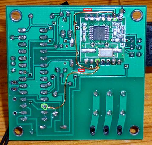
Modification of RFM12 power pin (PCB V1.0)
In PCBs >= V1.1, the RFM12 power pin is connected to an ATMega I/O pin to make it possible to restart the transceiver if communication fails.
If you want to modify your old PCB version to have this feature as well, cut two traces carefully (marked red in the picture) and connect two pins of the RFM transceiver to the ATMega (marked green in the picture).
Make sure you don't create a short circuit and cut the traces correctly. Use a multimeter to check this.
Modification of RFM12 power pin (PCB V1.1)
The PCB V1.1 has a fault in it's layout (not in the schematic though). Sadly, the ATMega PC3 pin is not only connected to power the RFM12, but is as well connected to the 3.3V line. Therefore the RFM12 has always power and the restart in case reception is not working anymore is not working like with the modified PCB 1.0 (see above).
To fix this, a copper trace needs to be cut at the point shown on the picture. If you do this modification, it's recommended to check with a multimeter that the RFM12 pin is not connected to 3.3V anymore, but to the PC3 pin of the ATMega.


