

Generic Maxi Speed
The Generic Maxi Speed PCB is a general purpose PCB specifically designed to support 5V operation voltage for the ATMega to allow it running at 20 MHz. But it can be used for other devices as well.
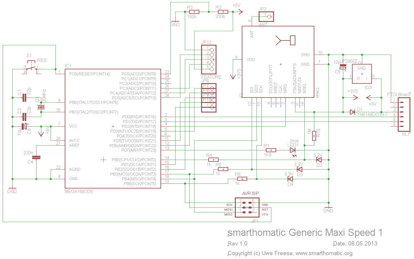
Schematics
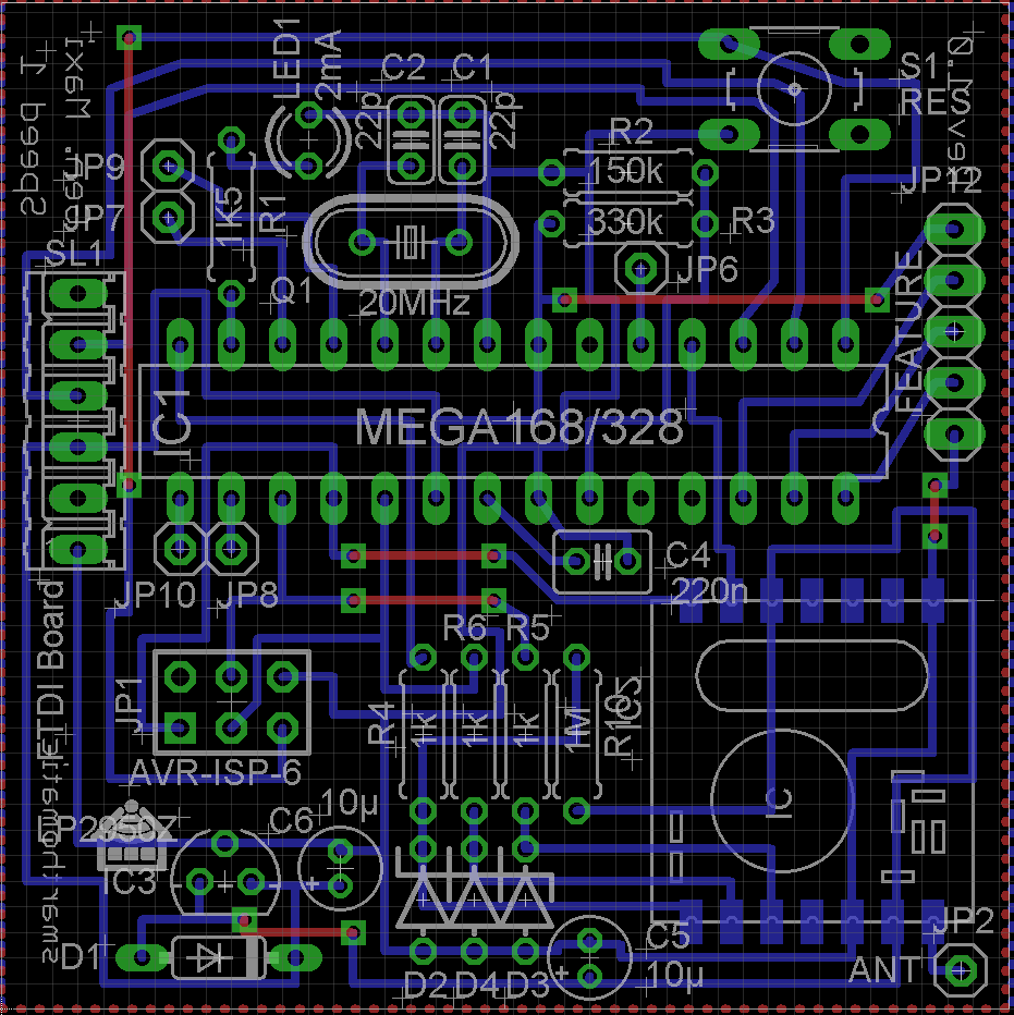
PCB Layout
Assembly Options
You can use several features of this PCB depending on if you assemble the parts or leave them out. Here's the list of assembly options you have.
Dual Voltage Support
The RFM12B modules can not run at a voltage of 5V. But this is needed to run the microcontroller at the highest possible clock frequency of 20 MHz. Therefore, the additional 3.3V voltage regulator (TS2950) is used. The high speed is especially useful to encrypt and decrypt the packets quickly.
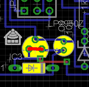
If you need this function, assemble TS2950, the 1N4148 diode and the capacitor next to them and use an operating voltage of 5V for the PCB (at the 6-pin connector).
If you don't need the function, leave the parts out and insert a bridge as marked red in the picture. You have to supply the operation voltage of 2.2V up to 3.8V then.
Quartz Crystal
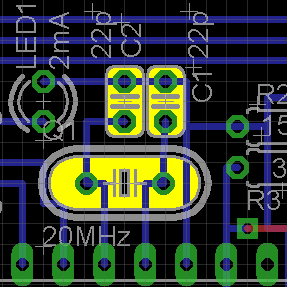
The crystal Q1 and the capacitors C1 and C2 can be used when the speed of the internal RC oscillatror (8 MHz) is not enough. This is the case e.g. for the base station. Look into the datasheet of the microcontroller for possible speeds at different operating voltages.
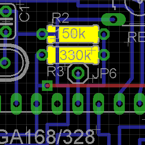
Battery Voltage Measurement
When using R2 and R3, you can measure the operating voltage at pin PC0 / ADC0. This is only useful for battery powered devices. The resistor values have to be changed according to the battery type and number of cells. The default values (150k and 330k) are correct for a device with two alkaline battery cells.
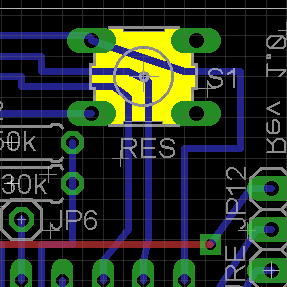
Reset Switch
The reset pin is useful when using the PCB as base station as as general purpose development device. You can restart the ATMega by pressing the button and without disconnecting the USB-to-serial adapter. For normal (battery powered) devices, it is probably enough to remove the battery shortly.
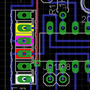
Serial Port and Power Pins
Power and serial port pins (RX, TX) are available on the connector for the USB-to-serial converter board. If you don't want to use the USB connection, you can directly connect +2.2..5V to pin 3 (red) and GND to pin 1 (white). A serial debug cable can be connected to pins 4 (RX, to MC, magenta) and 5 (TX, from MC, yellow).
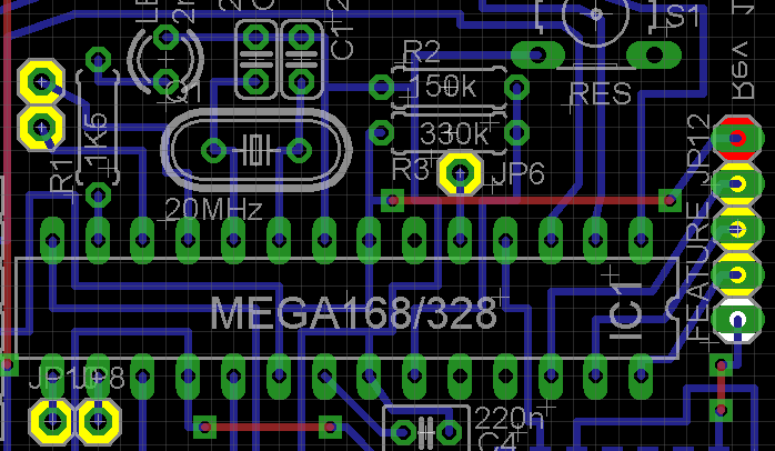
I/O pins with special abilities
For being useful for different use-cases, the I/O pins with special abilities were chosen to be available though connectors. These are:
- PC3 = ADC3
- PC4 = ADC4 = SDA (2-wire Serial Bus Data Input/Output Line)
- PC5 = ADC5 = SCL (2-wire Serial Bus Clock Line)
- PD5 = OC0B (PWM out)
- PD6 = OC0A (PWM out)
- PB1 = OC1A (PWM out)
- PB2 = OC1B (PWM out)
- PD3 = OC2B (PWM out) = INT1 (interrupt input, can wake up device)